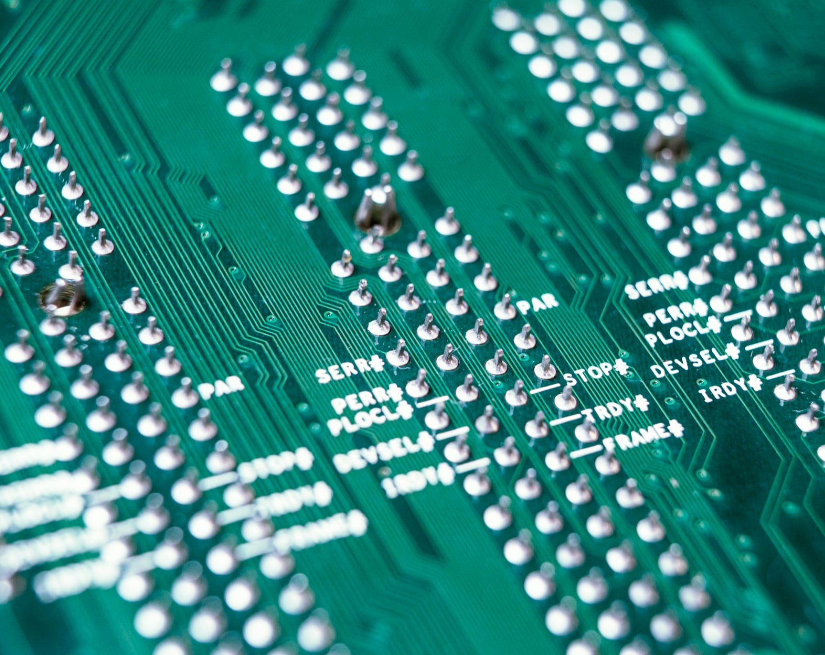
EKTOS designs professional Print Circuit Board Design – PCB layout for manufacturing, gives better EMC capabilities, higher yield during manufacturing, and easy to make future product design updates. Using the industry’s top design tools, we can support your needs for a highly professional ready-to-go solution based on data from your schematic entry.
We have accumulated more than 60 man-years of PCB layout experience with a huge variety in complexity. This ensures smooth and effective communication regardless of the type of PCB layout.
We can provide layout work fully or partly at our customer site. This is relevant for floor planning sessions, changes after EMC-test, etc.
WORLD-CLASS TOOLS
At EKTOS, we use a suite of the best tools and are open to taking in new tools upon reque st. The tools we currently use are:
OUR SKILLS and EXPERIENCE
We can offer a comprehensive set of skills:
- High-speed, multi-layer digital PCB designs: Bus routing, differential pairs, matched lengths
- Extensive RF and analog design: printed antennas, guard rings, RF shields, etc.
- Development of power electronics from a few watts to 100 kW
- Signal integrity issues to meet your digital design needs
- PCB layer management for signal integrity and impedance control
- DDR, DDR2, DDR3, SAS
- High-density SMT designs (BGA, uBGA, PCI, PCIE, CPCI, etc.)
- Flexible PCBs
- PCB with aluminum or ceramic substrate
- Complete assembly drawings
- Optimization for mass production
- Professional manufacturing documentation
SELECTED CASE STUDY
EKTOS develops control unit and wireless communication for the JHminiStrø feeding robot.
EKTOS has helped improve the new version of JHminiStrø in a number of ways..."
Lars Forbech,
Head of Development and Manufacturing
at JH Agro


